English (UK)
  日本語 (Japan)
  한국어 (Korean)
  Tiếng Việt
  中文 (Chinese)
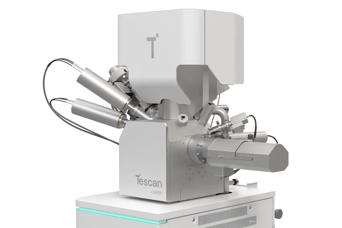
 TESCAN AMBER 2 is a precision Ga⁺ FIB-SEM platform engineered for high-resolution imaging, nanofabrication, and site-specific TEM lamella preparation. Built on TESCAN’s advanced Gallium Ion Column and Schottky FEG SEM optics, AMBER 2 delivers accurate beam control, outstanding milling repeatability, and superior surface finish on a wide variety of materials. With Intermediate Lens™, In-Flight Beam Tracing™, and unified TESCAN Essence™ software, the system enables seamless transitions between imaging and analytical conditions and supports recipe-driven automation for semiconductor failure analysis, materials research, and microelectronics R&D.
Focus Ion Beam Scanning Electron Microscopy (FIB-SEM)
Advanced FIB-SEM
for Insight and Impact
Precision, versatility, and unmatched performance, designed to meet the challenges of both routine and complex workflows. Whether you're working in materials science, life sciences,
or semiconductors, Tescan’s FIB-SEM systems provide more than high-resolution imaging. They give you the control to cut, shape,
and analyze structures with nanoscale accuracy.
From focused Ga-ion beams for fine detail to Xe plasma beams for fast volume processing, our modular platforms adapt to your needs. Combined with intuitive software and expert support, we help you move confidently from question to insight.
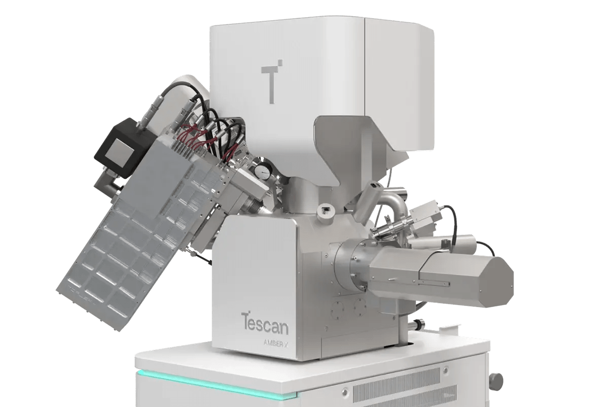
TESCAN AMBER X2 is a high-performance plasma FIB-SEM engineered for high-throughput, large-volume material removal and precise nano-machining across semiconductors, materials science, and multi-scale 3D analysis. Equipped with a Xenon plasma ion source, it achieves extremely high milling rates with minimal damage, supported by TruBeam™ ion optics for beam stability and TruSlice™ 3D tomography for volumetric reconstruction. Integrated TESCAN Essence™ software provides unified dual-beam control, automation, and scripting workflows — delivering consistent, reproducible performance from trenching to 3D imaging. AMBER X2 bridges productivity and analytical precision, supporting both routine and advanced correlative applications.
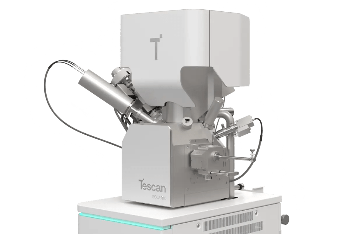
TESCAN SOLARIS 2 is a next-generation Ga⁺ FIB-SEM platform for precision nanofabrication, high-resolution imaging, and 3D analysis across semiconductor, materials, and nanotechnology applications. Featuring a Gallium LMIS and advanced TruBeam™ ion optics, SOLARIS 2 delivers superior beam stability, precise patterning, and reproducible nano-scale milling. Integrated Schottky FEG SEM optics with Intermediate Lens™ and In-Flight Beam Tracing™ provide analytical imaging with sub-nanometer resolution, while unified TESCAN Essence™ software ensures automated, consistent workflows from TEM lamella prep to 3D tomography.
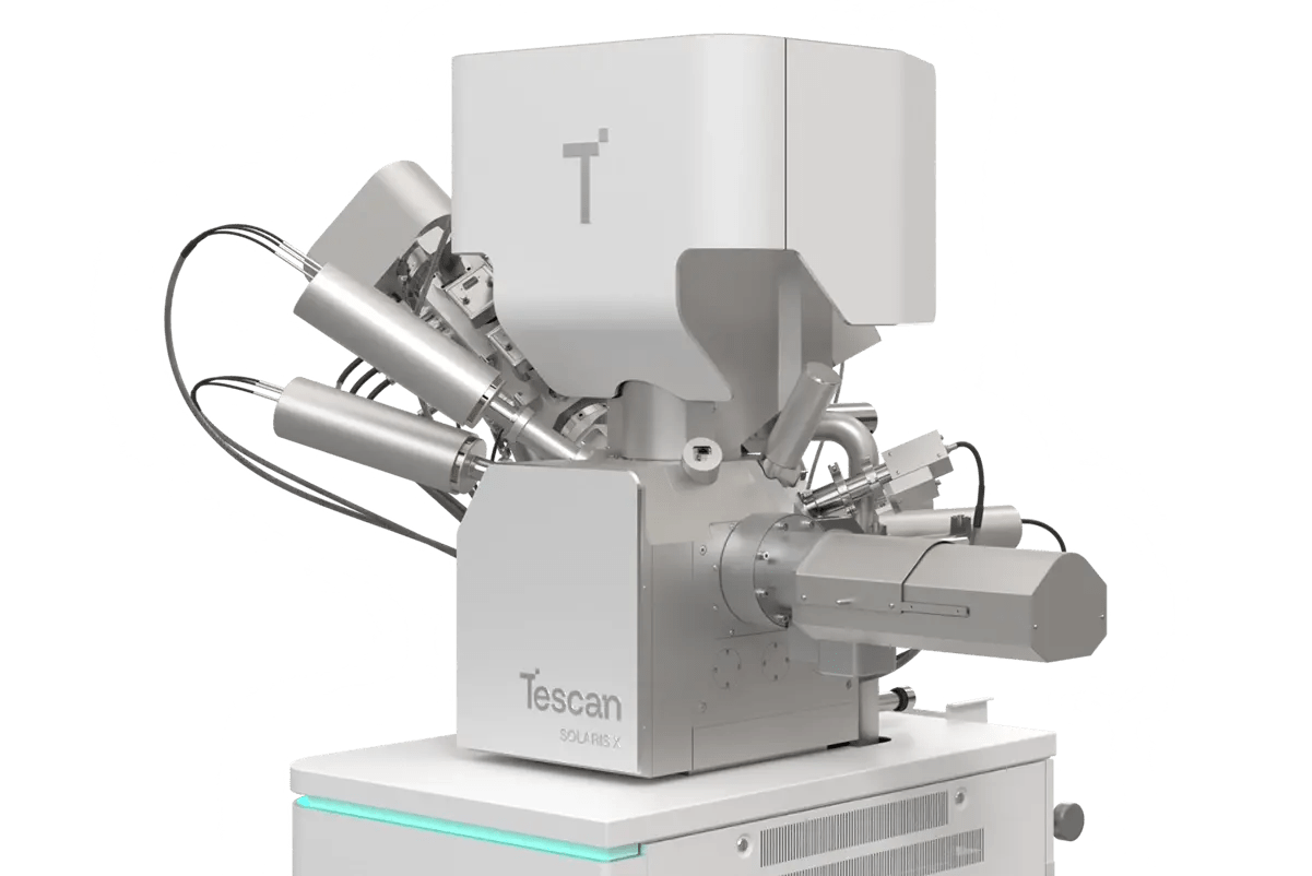
TESCAN SOLARIS X 2 is a next-generation Xe plasma FIB-SEM that combines unmatched throughput with analytical precision for large-volume milling, high-resolution imaging, and Ga-free TEM sample preparation. Built on the proven Mistral™ Xe plasma FIB column and advanced Triglav™ UHR SEM optics, SOLARIS X 2 delivers superior ion-beam stability, repeatability, and high-quality surface finish even at extreme currents. Unified TESCAN Essence™ automation provides recipe control and TruSlice™ 3D workflows for reproducible failure analysis, materials research, and semiconductor engineering.