English (UK)
  日本語 (Japan)
  한국어 (Korean)
  Tiếng Việt
  中文 (Chinese)
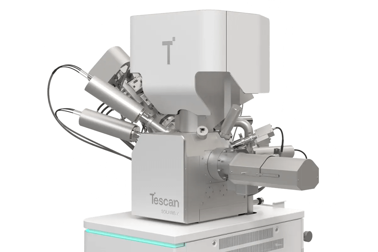
Introduction to TESCAN SOLARIS X 2
TESCAN SOLARIS X 2 is a Xe plasma FIB-SEM platform engineered for high-throughput nano-machining, Ga-free TEM sample preparation, and large-volume 3D analysis. With the Mistral™ plasma column and Triglav™ UHR SEM optics, it provides fast, uniform milling and stable, high-contrast imaging at low kV. Essence™ software unifies SEM/FIB control, automation, and TruSlice™ 3D tomography for consistent results across extended workflows.
Typical Applications
- Semiconductor FA & packaging: large cross-sections, TSV/die-stack exposure, delamination and void inspection.
- Ga-free TEM preparation: rapid trenching, lift-out, thinning and final polish without ion contamination.
- Advanced materials: large-area trenching, interface studies and microstructure mapping.
- Additive manufacturing & metallurgy: porosity and layer-wise evaluation, 3D reconstruction of printed parts.
- Life science & geoscience: high-contrast 3D imaging of porous/biological samples at low beam damage.
Key Features
High-Throughput Xe Plasma Ion Beam
- Xenon plasma ion source enables removal rates far beyond Ga FIB for fast bulk mill and large volumes.
- Stable beam at high currents supports uniform trenching and clean surfaces for tomography or TEM prep.
- Low contamination pathways suitable for Ga-free workflows.
Mistral™ Plasma Column & Dual-Beam Geometry
- Optimized column design for precise ion–electron coincidence at working tilt.
- Uniform sputtering performance across current setpoints with reduced redeposition.
Triglav™ UHR SEM Optics
- Schottky FEG with three-lens Triglav™ optics delivers sub-nanometer resolution and stable contrast at low kV.
- Wide field and depth of focus simplify navigation over large or complex samples.
Essence™ Automation & TruSlice™ 3D Tomography
- Unified SEM/FIB control with recipe editor, macros and scripting for unattended runs.
- TruSlice™ 3D synchronizes serial sectioning and imaging for accurate volume reconstruction.
Analytical & Correlative Integration
- Supports EDS, EBSD, WDS, CL, STEM-in-SEM and cryo-correlative options.
- Compatible with nanomanipulation and in-situ stages for dynamic experiments.
Flexible Vacuum & Sample Environment
- High-vacuum operation for clean analytics; variable pressure (1–700 Pa) for charging/porous materials.
- Spacious chamber with multi-port layout for detectors and automation accessories.
Representative Technical Specifications
| Specification | Value (representative) |
|---|---|
| Ion source | Xenon plasma ion source |
| Ion beam energy | 1 – 30 keV |
| Ion beam current range | 1 nA – > 2 µA |
| SEM electron source | High-brightness Schottky FEG |
| SEM accelerating voltage | 200 eV – 30 keV |
| SEM resolution | 1.2 nm @ 30 keV (SE); 3.5 nm @ 1 keV (In-Beam SE) |
| Ion beam resolution | < 20 nm @ 30 keV |
| Vacuum modes | High Vacuum; Variable Pressure (1 – 700 Pa) |
| Detectors (standard) | SE, BSE, STEM-in-SEM, ion BSE; optional EDS, EBSD, WDS, CL |
| Software platform | TESCAN Essence™ with TruSlice™ 3D, automation and scripting |
*Specifications may vary depending on configuration and installed options.
FAQ
What makes SOLARIS X 2 different from Ga FIB systems?
The Xenon plasma source delivers far higher milling rates and Ga-free sample preparation, ideal for advanced packaging and large-volume 3D applications.
Can SOLARIS X 2 perform fully automated 3D tomography?
Yes. TruSlice™ 3D coordinates serial sectioning and SEM imaging to produce accurate, drift-corrected volumes.
Is SOLARIS X 2 suitable for Ga-free TEM sample preparation?
Yes. Xe plasma milling supports fast trenching and high-quality final surfaces without Ga implantation.
How is beam stability maintained during long milling sessions?
The Mistral™ column and optimized ion optics stabilize beam shape and current for uniform milling over extended runs.
Does SOLARIS X 2 support analytical and correlative workflows?
Yes. It integrates EDS, EBSD, WDS, CL and STEM-in-SEM, and is compatible with cryo, CLEM and in-situ stages.
Overview of TESCAN SOLARIS X 2
TESCAN SOLARIS X 2 unites high-throughput Xe plasma milling with Triglav™ UHR SEM imaging and Essence™ automation. It accelerates time-to-data for failure analysis, semiconductor engineering and materials research while ensuring Ga-free preparation and reliable 3D results.
Related Video / Webinar
- Webinar: -
- Video: -
Contact & Support