English (UK)
  日本語 (Japan)
  한국어 (Korean)
  Tiếng Việt
  中文 (Chinese)
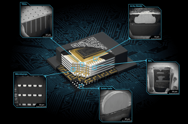
M.SEMICON delivers advanced inspection, measurement, and failure analysis solutions for the fast-growing semiconductor and electronics industry in Vietnam. We support customers across the entire product lifecycle, from research & development (R&D) and quality assurance/quality control (QA/QC) to in-depth failure analysis (FA).
With a team of experienced engineers and state-of-the-art instruments, M.SEMICON combines global technologies with localized services, helping clients shorten time-to-market and strengthen their competitiveness.
Scope of Solutions
1. Electron Microscopy & Microanalysis
- Purpose: Imaging morphology and microstructure, analyzing elemental composition and crystallography for QC and FA.
- Representative Equipment: SEM (conventional/FE), FIB-SEM, STEM/TEM, EDS/EBSD/WDS, CL/EBIC.
2. Surface & Thin-Film Characterization
- Purpose: Measuring film thickness, roughness, stress, optical parameters, and wafer geometry for thin-film process optimization.
- Representative Equipment: Ellipsometer/reflectometer, stylus or optical profilometer, AFM, interferometer, wafer bow/warp/TTV metrology.
3. Elemental & Trace Contamination Analysis
- Purpose: Determining bulk and trace elemental composition, detecting contamination on wafers, UPW, and process chemicals.
- Representative Equipment: XRF, micro-XRF (mapping), TXRF (wafer surface contamination), ICP-MS/ICP-OES, GD-OES.
4. Advanced Surface & Chemical Analysis
- Purpose: Characterizing chemical states, ultra-thin films, polymers, organic/inorganic contamination, and crystallinity.
- Representative Equipment: XPS, AES, SIMS/TOF-SIMS, FTIR, Raman spectroscopy, XRD.
5. Wafer Defect Inspection & Process Metrology
- Purpose: Detecting wafer defects early, monitoring lithography and film parameters to ensure yield and process stability.
- Representative Equipment: Wafer inspection systems (brightfield/darkfield/e-beam), CD-SEM, scatterometry (OCD), overlay metrology, inline CMP/etch/PVD metrology.
6. PCB/SMT Inline Inspection
- Purpose: Ensuring soldering, assembly, and PCB quality in electronics manufacturing.
- Representative Equipment: SPI, AOI, AXI, ICT/flying-probe, acoustic microscopy (C-SAM), reflow profiling.
7. Functional Testing & Automated Test Equipment (ATE)
- Purpose: Verifying IC, module, and board-level performance and compliance before shipment.
- Representative Equipment: SoC/Memory ATE, board-level testers (ICT, boundary-scan, functional test), handlers (with thermal forcing), RF/mmWave/OTA testers.
8. Failure Analysis Systems
- Purpose: Isolating and identifying root causes of electrical, structural, or functional failures.
- Representative Equipment: Sample preparation tools (ion milling, plasma FIB, decapsulation), photon emission microscopy (PEM), OBIRCH/TIVA/LIVA, lock-in thermography, micro/nano-probing.
9. Cleanroom & Contamination Control
- Purpose: Maintaining ISO-class cleanroom standards, preventing airborne, chemical, and electrostatic contamination.
- Representative Equipment: Particle/AMC monitoring systems, TOC analyzers, ion chromatography, liquid particle counters (UPW/chemicals), ESD/EOS testers.
10. Reliability & Environmental Testing
- Purpose: Evaluating durability, reliability, and lifetime of ICs, modules, and boards under harsh operating conditions.
- Representative Equipment: HTOL, HAST, temperature cycling/shock testers, burn-in systems, power cycling, vibration/shock testers, IR thermography.
Key Benefits
- Higher Product Reliability & Yield
Early detection of defects and process deviations helps reduce latent failures, improve device reliability, and increase manufacturing yield. - Comprehensive Failure Analysis & Root Cause Elimination
Advanced FA workflows and sample prep tools allow fast isolation of failure mechanisms, enabling permanent corrective actions. - Optimized Manufacturing Costs & Cycle Time
Minimize scrap, rework, and downtime through inline/near-line inspection and process monitoring, accelerating time-to-market. - Process & Quality Standardization
Ensure consistent product quality across production lines, meeting ISO, JEDEC, and automotive (IATF16949) requirements. - Support for R&D & Technology Innovation
Enable faster material characterization, process development, and new product introduction with state-of-the-art tools. - Digital Integration & Smart Manufacturing Readiness
Seamless connectivity with MES/ERP systems, SPC/YMS analytics, and data-driven decision-making for Industry 4.0 initiatives. - Regulatory & Global Compliance
Support for environmental monitoring, contamination control, and qualification testing aligned with international supply chain standards. - Local Expertise & Lifecycle Service
Dedicated Vietnam-based engineering team for consultation, installation, training, preventive maintenance, and rapid on-site support. - Scalability & Future-Proof Investment
Modular and upgradeable solutions that can grow with production capacity and adapt to next-generation technologies.
Target Customers
- Semiconductor Fabs & OSAT/ATP Facilities
Wafer fabrication, assembly & packaging, probe/test houses requiring inline metrology, defect inspection, and yield enhancement tools. - SMT/PCB & Module Manufacturers
Electronics assembly, board makers, EMS/ODM/OEM facilities needing SPI, AOI, AXI, ICT, and functional test solutions. - Fabless & IDMs
Design houses and IDMs with in-house characterization, reliability, and FA labs supporting product development and qualification. - Automotive & Industrial Electronics
Tier 1/2 suppliers for automotive ECU, sensors, power modules, industrial controllers demanding reliability & environmental testing. - Research Institutes & Universities
Academic and government labs in materials science, microelectronics, and advanced packaging doing R&D and training. - QA/QC, FA & Reliability Departments
Teams responsible for quality assurance, root cause analysis, and regulatory compliance across production lines. - Cleanroom & Contamination Control Teams
Facilities managing ISO-class cleanrooms, UPW systems, and AMC monitoring to prevent yield loss.