English (UK)
  日本語 (Japan)
  한국어 (Korean)
  Tiếng Việt
  中文 (Chinese)
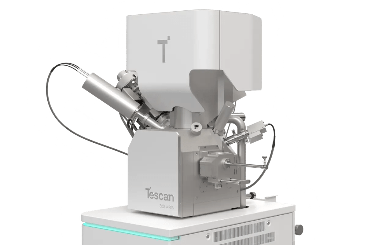
Introduction to TESCAN SOLARIS 2
TESCAN SOLARIS 2 is a state-of-the-art Ga⁺ FIB-SEM platform designed for precision nanofabrication, high-resolution imaging, and 3D analysis across a wide range of semiconductor and materials-science applications. Its Gallium Liquid Metal Ion Source (LMIS) and TruBeam™ ion optics enable high-stability, precise milling and patterning. The Schottky FEG SEM column with Intermediate Lens™ and In-Flight Beam Tracing™ provides stable analytical imaging. Unified Essence™ software delivers automation, scripting, and correlative workflows for efficient sample preparation and analysis.
Typical Applications
- Semiconductor R&D and FA: site-specific cross-sections, device modification, TEM lamella prep, and circuit probing.
- Nanotechnology & materials research: nano-patterning, defect isolation, and 3D tomography with high precision.
- TEM sample preparation: automated trenching, lift-out, thinning and final polishing with minimal damage.
- Failure analysis & packaging: delamination, via/TSV inspection, and void/interface evaluation.
- Correlative & in-situ studies: integration with cryo-transfer, Raman, CL, or STEM detectors for multi-modal analysis.
Key Features
High-Precision Gallium Ion Beam
- Gallium LMIS provides a finely focused beam for accurate milling, nano-patterning and TEM sample preparation.
- Beam current range from sub-pA to > 50 nA covers delicate polishing to high-speed trenching.
- Optimized beam shape ensures smooth, artifact-free surfaces even at low currents.
TruBeam™ Ion Optics
- Enhanced beam stability and reduced aberrations for long-duration nano-machining.
- Dynamic charge compensation minimizes drift and redeposition during complex patterning.
Advanced Electron Optics
- Schottky FEG SEM column with Intermediate Lens™ and In-Flight Beam Tracing™ ensures stable resolution across probe currents.
- High-contrast SE/BSE imaging supports precise end-point detection and structural characterization.
Automation and TESCAN Essence™
- Unified SEM/FIB control with recipe editor and scripting interface.
- TESCAN Auto FIB automates lamella prep, serial sectioning and 3D workflows.
3D Tomography and Correlative Imaging
- Serial FIB slicing synchronized with SEM imaging for accurate 3D reconstruction.
- Compatible with third-party visualization tools for volume rendering and analysis.
Flexible Analytical Integration
- Supports EDS, EBSD, WDS, CL and STEM-in-SEM.
- Cryo, nanomanipulation and in-situ heating extend experiment capabilities.
Representative Technical Specifications
| Specification | Value (representative) |
|---|---|
| Ion source | Gallium Liquid Metal Ion Source (LMIS) |
| Ion beam energy | 1 – 30 keV |
| Ion beam current range | sub-pA – > 50 nA |
| SEM electron source | High-brightness Schottky FEG |
| SEM accelerating voltage | 200 eV – 30 keV |
| SEM resolution | 1.2 nm @ 30 keV (SE); 3.5 nm @ 1 keV (In-Beam SE) |
| Ion beam resolution | < 15 nm @ 30 keV |
| Vacuum modes | High Vacuum; Variable Pressure (1–700 Pa) |
| Detectors (standard) | SE, BSE, In-Beam SE/BSE, STEM-in-SEM; optional EDS, EBSD, CL |
| Software platform | TESCAN Essence™ with Auto FIB, recipe editor and scripting |
*Specifications may vary depending on configuration and installed options.
FAQ
What distinguishes SOLARIS 2 from previous Ga FIB-SEM systems?
SOLARIS 2 features new TruBeam™ optics and Essence™ automation, offering superior beam control, higher precision and fully automated TEM and 3D workflows.
Can SOLARIS 2 prepare TEM lamellae automatically?
Yes. Auto FIB recipes automate trenching, lift-out, thinning and final polishing, producing high-quality lamellae with minimal user input.
How does SOLARIS 2 ensure stability for long patterning sessions?
TruBeam™ optics dynamically compensate for charge build-up and drift, maintaining consistent focus and accuracy over time.
Does SOLARIS 2 support 3D FIB-SEM tomography?
Yes. Automated serial slicing with SEM imaging enables 3D reconstruction and quantitative volume analysis at the nanoscale.
Can SOLARIS 2 be integrated with analytical and correlative tools?
Yes. It supports EDS, EBSD, WDS, CL and STEM-in-SEM, as well as cryo and Raman modules for multi-modal workflows.
Overview of TESCAN SOLARIS 2
TESCAN SOLARIS 2 combines Ga⁺ FIB precision with advanced SEM optics and Essence™ automation, streamlining TEM sample preparation, 3D tomography and nano-machining for semiconductors and materials research. It sets a new standard for accuracy, reliability and productivity in dual-beam nanoscience systems.
Related Video / Webinar
- Webinar: -
- Video: -
Contact & Support