English (UK)
  日本語 (Japan)
  한국어 (Korean)
  Tiếng Việt
  中文 (Chinese)
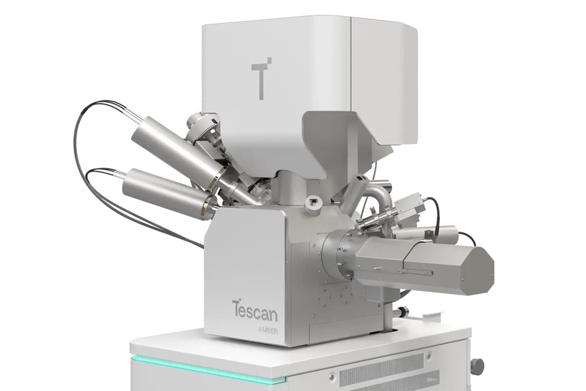
Introduction to TESCAN AMBER 2
TESCAN AMBER 2 is a precision Ga⁺ FIB-SEM platform designed for high-resolution imaging, nanofabrication, and site-specific TEM lamella preparation. Built upon TESCAN’s advanced Gallium Ion Column and Schottky FEG SEM optics, AMBER 2 offers accurate beam control, outstanding milling repeatability, and superior sample quality. With Intermediate Lens™, In-Flight Beam Tracing™, and unified TESCAN Essence™ software, it ensures smooth transitions between imaging and analytical modes, supporting automated workflows for semiconductor failure analysis, materials research, and microelectronics R&D.
AMBER 2 further benefits from a dual-beam geometry with a 5-axis eucentric stage to maintain region-of-interest alignment during tilting and rotation, integrated endpointing for precise cross-section control, and optional Auto FIB workflows that standardize trenching, lift-out, thinning, and final polish. Optional serial sectioning synchronized with SEM imaging provides a path to 3D FIB-SEM tomography, while a broad accessory ecosystem (STEM-in-SEM, EDS, EBSD, CL, nanomanipulation, cryo) enables correlative experiments and repeatable results across users and labs.
Typical Applications
- Semiconductor FA & device engineering: precision cross-sections, contact/via exposure, circuit probing and edits.
- TEM lamella preparation: site-specific thinning, lift-out and final polish for high-quality electron transparency.
- Nanoscale materials research: trenching, nano-patterning, phase/defect localization with correlative SEM/EDS/EBSD.
- 3D FIB-SEM tomography: serial slicing and SEM imaging for sub-micron volume reconstruction.
- Microsystems & packaging: TSV/µ-bump inspection, delamination/void analysis, interface characterization.
Key Features
Precision Gallium FIB for Site-Specific Milling
- Ga LMIS with stable beam formation for accurate cross-sections, undercuts and polish steps.
- Wide ion-current capability (from sub-pA for gentle cleaning to tens of nA for faster trenching) to balance speed and surface fidelity.
Optimized Dual-Beam Geometry & Eucentric Stage
- Electron/ion columns arranged for clear views at working tilt; the 5-axis eucentric stage keeps features in view during milling/imaging.
- Robust drift control and active compensation support long unattended runs.
TESCAN Essence™ Automation & Recipes
- Unified SEM/FIB control with guided recipes for cross-sectioning, TEM lamella prep and multi-site jobs.
- Scripting and batch execution reduce operator workload; advanced endpoints improve consistency.
3D Serial Sectioning & Analytics
- Optional serial milling synchronized with SEM imaging for volume reconstruction and quantitative morphometrics.
- Correlate morphology (SE/BSE), composition (EDS) and crystallography (EBSD) across slices.
Electron Optics & Detectors
- Schottky FEG SEM with aperture-less optics (Intermediate Lens™ + In-Flight Beam Tracing™) for stable resolution across probe currents.
- Detector suite for SE/BSE/In-Beam; options for STEM-in-SEM, EDS, EBSD, CL and ion signal acquisition.
Flexible Sample Environments
- High vacuum imaging for uncompromised analytics; variable pressure modes support charging/porous materials.
- Compatibility with cryo-transfer and nanomanipulators for delicate samples and lift-out workflows.
Representative Technical Specifications
| Specification | Value (representative) |
|---|---|
| Ion source | Gallium LMIS (Ga) |
| Ion beam energy | 1–30 keV (typical) |
| Ion beam current range | sub-pA – > 50 nA |
| SEM electron source | High-brightness Schottky FEG |
| SEM accelerating voltage | 200 eV – 30 keV |
| SEM resolution (rep.) | ~1.2 nm @ 30 keV (SE); ~3.5 nm @ 1 keV (In-Beam SE) |
| Vacuum modes | High Vacuum; Variable Pressure (rep. 1–700 Pa) |
| Stage | 5-axis motorized (X/Y/Z/tilt/rotation), eucentric geometry |
| Detectors (typical) | SE, BSE, In-Beam SE/BSE, STEM-in-SEM; options for EDS, EBSD, CL |
| Automation | TESCAN Essence™ recipes (cross-section, TEM lamella), scripting, serial sectioning |
*Specifications are representative and may vary with configuration and installed options.
FAQ
How does AMBER 2 differ from a plasma FIB (PFIB)?
AMBER 2 uses a Ga LMIS for maximum precision and excellent surface finish — ideal for site-specific edits and lamella prep. PFIBs (xenon) mill faster on very large areas but are not always necessary for fine device work.
Can AMBER 2 prepare TEM lamellae end-to-end?
Yes. Guided recipes cover trenching, lift-out, thinning and final polish; nanomanipulator and gas injection support are available.
What 3D capabilities does AMBER 2 offer?
Optional serial milling plus SEM imaging enables FIB-SEM tomography of sub-micron volumes with correlative EDS/EBSD.
How does Essence™ automation improve repeatability?
Recipe-based automation in Essence™ standardizes beam parameters, milling depth and imaging conditions to ensure consistent geometry and reproducible results across operators or sample types.
How is cross-beam alignment maintained during long sessions?
AMBER 2 employs auto-alignment routines and eucentric stage geometry to keep ion and electron beams intersecting precisely at the region of interest, minimizing drift during extended patterning or serial sectioning runs.
Overview of TESCAN AMBER 2
TESCAN AMBER 2 delivers the precision of Ga FIB with modern automation for repeatable nano-machining and sample preparation. Unified SEM/FIB control, recipe-based workflows and optional 3D serial sectioning provide an efficient path from site-specific milling to nanoscale analysis across semiconductors, packaging and advanced materials.
Related Video / Webinar
- Webinar: -
- Video: -
Contact & Support