TESCAN AutoSlicer™ - Robust and reliable semi-automated TEM sample preparation
 Key Benefits:
-
Prepare high quality, ultra-thin TEM samples from sub-10 nm semiconductor technology nodes in less than one hour using advanced dedicated workflows provided by optimized TESCAN Ga FIB-SEM platform
-
Improve sample preparation throughput with fully automated TEM lamella preparation to the undercut in the trench followed by a guided workflow for semiautomated attachment of the lamella to the TEM grid
-
Retain flexibility for advanced TEM lamella preparation thanks to our nanomanipulator in the “below FIB” position, which allows preparation of top-down, planar and inverted lamella geometries without need of a flipping device
-
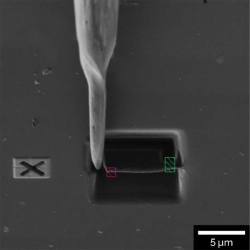
Obtain robust, predictable results on large variety of samples using adjustable reference marks that best suit the sample and its structure
-
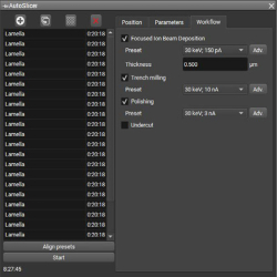
Develop custom workflows unique to the samples processed in your lab. User-defined parameters for the automated TEM sample and crosssection preparation can be saved as guided workflows to help assure all samples meet the quality requirements for the type of analysis
-
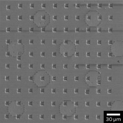
Perform multi-site, unattended TEM sample preparation from multiple areas of interest with TESCAN AutoSlicer`s option to specify an array of lamellae at different locations and from multiple samples, preparing all samples in a single batch operation
-
TESCAN AutoSlicer™ is compatible with all TESCAN Ga and Plasma FIB-SEM instruments
Applications:
-
Prepare ultra-thin TEM lamellae, with the minimum amorphous damage from 10 nm FinFET devices
-
High-throughput cross-sectioning, analysis and sample preparation for logic, memory, RF/power compound semiconductors (GaN/SiC) and many other types of semiconductor devices


 English (UK)
  日本語 (Japan)
  한국어 (Korean)
  Tiếng Việt
  中文 (Chinese)


