English (UK)
  日本語 (Japan)
  한국어 (Korean)
  Tiếng Việt
  中文 (Chinese)
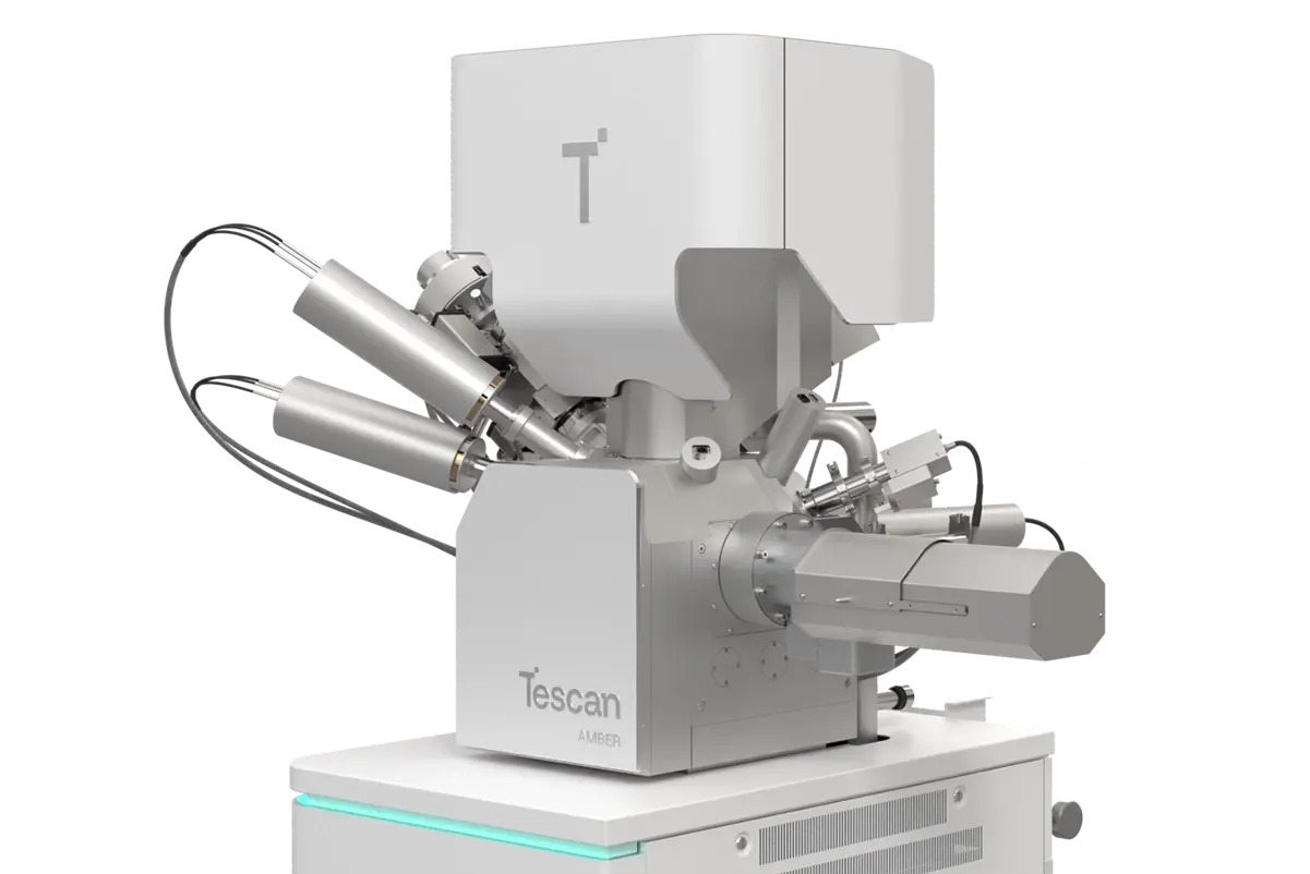
Automated Ga⁺ FIB-SEM platform for high-precision TEM sample prep and nanoscale prototyping.
Tescan AMBER integrates BrightBeam™ field-free SEM optics with the Orage™ Ga⁺ FIB and fully automated lamella workflows. Designed for versatility, it supports inverted and planar sample prep, nanoprototyping, and gentle final polishing across a wide range of material types.
How AMBER 2 Empowers Your Research
TESCAN AMBER 2 is a fully automated Ga FIB-SEM for routine TEM sample preparation, nanoscale characterization, and prototyping.
Offering precision and ease of use, it delivers exceptionally high FIB image quality even at low accelerating voltages. The field-free BrightBeam™ SEM column ensures high contrast nanoscale imaging and exceptional sample versatility.
Whether preparing TEM samples, creating nanostructures, or characterizing nanomaterials, AMBER 2 is the perfect tool for a variety of use cases.
-
Automated TEM Preparation: Prepare high-quality TEM samples automatically with minimal damage.
-
Advanced TEM Lamella Preparation: Achieve excellent quality, optimal geometry and minimal amorphization damage in TEM samples.
-
FIB Nanoprototyping: Fabricate, create or modify materials into functional devices using a single FIB-SEM instrument.
-
Advanced SEM Contrast Methods: Enhance surface sensitivity and detect different phases more effectively.
-
Electron Beam Lithography: Craft precise functional prototypes at nano and micro scales with TESCAN own Electron Beam Lithography and Fast Beam Blanker.
-
User-friendly: Obtain high-quality data without needing extensive FIB-SEM expertise.
Key benefits of AMBER 2
Automate your TEM sample preparation workflow with TESCAN AMBER 2, a field-free Ga FIB-SEM system offering an easy, dependable solution for automated and versatile TEM specimen preparation.
-
Explore new TEM possibilities by preparing inverted or planar samples and transferring them to the grid with a nanomanipulator for precise feature orientation.
-
Fabricate, create, or modify functional devices with AMBER 2’s capabilities for electron beam lithography, ion beam prototyping, FEBID, or FIBID, enhancing design flexibility and creativity.
-
Simplify FIB-SEM operation with TESCAN Essence™ software, automating SEM and FIB alignments and providing advanced stage collision protection for all skill levels.
-
Perform ultra-high-resolution imaging and nanoanalysis on diverse materials with the BrightBeam™ field-free UHR-SEM column and high current Orage™ FIB column, ensuring excellent performance and versatility.
-
Gain deeper material insights with AMBER’s multimodal detection system, enabling simultaneous acquisition of multiple signals.