English (UK)
  日本語 (Japan)
  한국어 (Korean)
  Tiếng Việt
  中文 (Chinese)
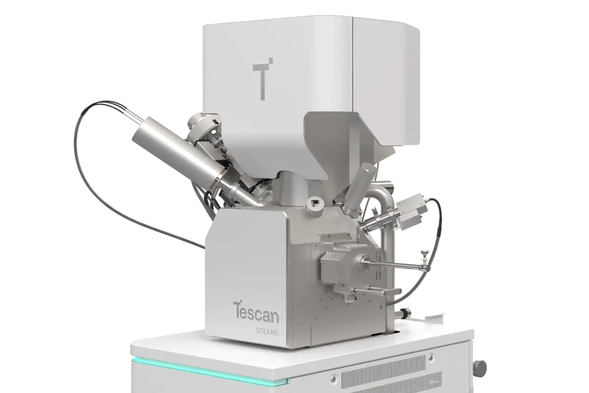
Dedicated Ga⁺ FIB-SEM for automated, high-precision TEM sample prep in semiconductor applications.
TESCAN SOLARIS is a fully automated sample prep platform optimized for advanced devices with sub-10 nm features. It integrates the Triglav™ SEM, AutoTEM Pro™ software, and OptiLift™ nanomanipulator to enable hands-free, repeatable lamella prep in planar, inverted, or top-down geometries.
Advanced TEM Lamella Preparation for Modern Semiconductor Laboratories
TESCAN SOLARIS 2 is a fully automated Ga FIB-SEM designed for high-precision TEM lamella preparation, equipped with AI-driven TEM AutoTEM Pro™ software. Engineered for applications in Failure Analysis, R&D, and Quality Control, SOLARIS 2 seamlessly integrates advanced SEM and FIB alignments, ensuring consistent system readiness and reducing time to data.
It excels in handling a wide range of electronic devices, including the latest in logic, memory, power, and display technologies, providing reliable performance for your most demanding sample preparation needs.
Precision Without Compromise
SOLARIS 2 delivers exceptional FIB resolution with minimal beam damage and milling artifacts. It’s not just for standard (top-down) lamella - you’ll also master inverted, planar, and double-cross lamella with our optimized single-step in-situ lift-out geometries, ensuring your samples are ready with precision and efficiency.
Ga FIB Meets UHR-SEM Immersion Optics
Experience the powerful combination of Ga-focused ion beam and ultra-high-resolution SEM immersion optics. This integration ensures top-tier performance in ion beam milling and SEM end-pointing, offering unmatched surface sensitivity and contrast, even on the most complex semiconductor samples.
Maximize Your TEM Sample Preparation with SOLARIS 2
-
Intelligent Automation: Automatically craft high-quality TEM samples with minimal damage, hands-free.
-
Advanced Flexibility: Adapt to any lamella geometry with exceptional quality and reduced amorphization.
-
Precision Targeting: Achieve unparalleled surface sensitivity and material contrast across diverse electronic devices and structures.
-
Consistent Readiness: Get repeatable, high-quality results without lengthy alignments or setups.
-
Customizable Workflows: Seamlessly switch between semi-automated and fully automated sample prep tailored to your specific needs.
-
Intuitive Operation: Obtain superior data quality with ease, regardless of your FIB-SEM expertise.
Main Benefits of TESCAN SOLARIS 2
-
Fast, Precise TEM Samples: Produce ultra-thin TEM samples from sub-10 nm nodes in under an hour with TESCAN TEM AutoPrep™ Pro. Fully automated from lift-out to final FIB polishing, it delivers consistently superior results every time.
-
Pinpoint Accuracy for Advanced Devices: Target single transistor lines in GAA or FinFET devices with pinpoint accuracy using AI-driven fiducial mark recognition and high-resolution imaging from the Triglav™ SEM column featuring advanced SE and BSE detectors for enhanced contrast at the beam coincident point.
-
Adaptable Lamella Prep with OptiLift™: Prepare top-down, planar, and inverted lamella effortlessly with the OptiLift™ nanomanipulator, strategically placed “below FIB.” This innovative design eliminates the need for extra flipping devices, simplifying your workflow.
-
Always Ready, Always Aligned: Keep your system ready with automated electron and ion column alignments that run overnight, ensuring minimal setup and maximum uptime.
-
High-Resolution Imaging Excellence: The Triglav™ SEM column, designed for ultra-high-resolution imaging, delivers outstanding surface sensitivity and contrast, making it ideal for beam-sensitive materials.
-
Streamlined Productivity: The redesigned TESCAN TEM AutoPrep™ Pro offers intuitive navigation between processes and extensive customization for any TEM lamella workflow, boosting productivity for every user.